

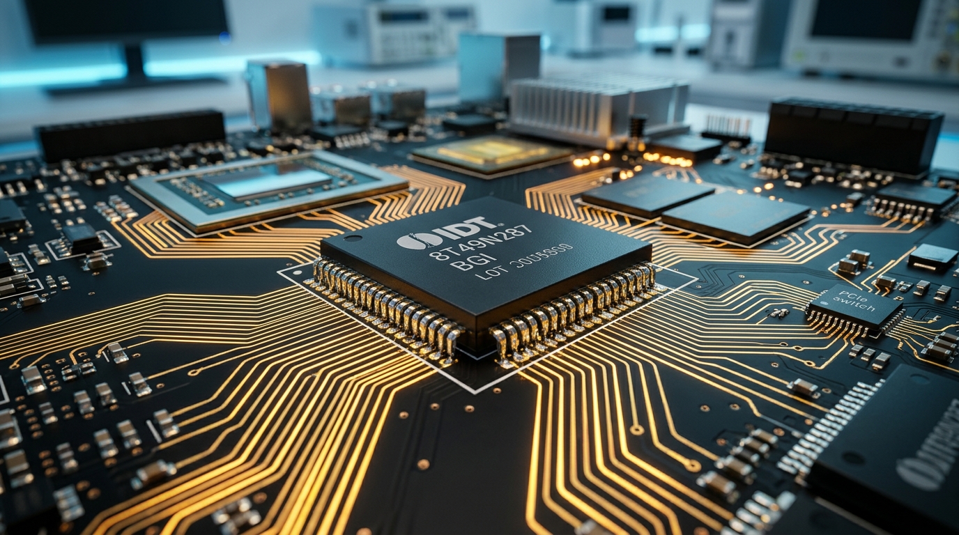
Core Foundations of Integrated Device Technology.
Integrated device technology drives speed in silicon hardware. Server boards link CPUs, RAM, and AI chips. Without clean timing, data bits collide on traces. Integrated device technology delivers timing chips. It supplies jitter cleaners and PCIe switches. These mixed-signal chips sync server racks. Teams keep noise low to stop bit loss. Reviewing shifts in chip industry manufacturing shows how packaging impacts yield. Clean clock trees protect system uptime.
Key Engineering Targets.
- Jitter Limits: Keep PCIe Gen 5 clock jitter below 150 femtoseconds.
- Clock Trees: Use dual-loop PLLs. Clean input clock phase noise.
- Signaling Standards: Deploy LP-HCSL drivers with on-chip loads.
- Domain Isolation: Route split clocks using SRIS setups.
The Shift to Active Silicon Timing.
Early motherboards relied on simple quartz crystals. Those crystals fed raw clock pulses to CPUs. As bus speeds passed 100 MHz, trace delays caused skew. Integrated device technology solved this limit. It uses active clock fan-out chips.
Silicon chips combine analog PLLs with digital dividers. Mixed-signal chips multiply base clock rates into gigahertz ranges. They buffer signals to board endpoints. They keep picosecond edge matching. Server blades need this precision. It keeps serial links fast and clean.
Understanding Jitter Physics and Phase Noise.
Clock jitter represents tiny timing errors in signal edges. A perfect clock transitions at exact intervals. In real silicon, heat alters transition times. Power shifts also add phase noise. This small variation is phase jitter.
Teams split jitter into two forms. Random jitter comes from thermal physics in the die. Deterministic jitter comes from power rail ripple and cross-talk. When jitter rises, the data eye closes on receivers. Bit error rates surge. High errors force links to drop to slower bus speeds.
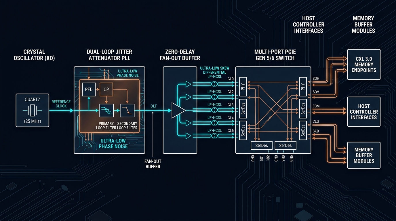
Figure 1.0: High-performance integrated device timing architecture detailing crystal reference input, dual-loop jitter cleaning, fan-out buffers, and multi-port PCIe switch distribution.
Clock Tree Design: Jitter Cleaners and Fan-Out Buffers.
Server systems build structured clock trees. They route timing across wide boards. A primary crystal feeds a central jitter cleaner. That cleaner filters incoming noise. It drives downstream fan-out buffers. Each buffer feeds a dedicated block like PCIe switches or memory controllers.
Dual-Loop Phase-Locked Loop Design.
High-end timing chips use two cascaded PLLs. The first loop uses a narrow bandwidth filter. It locks to a noisy input clock. It strips away high-frequency phase jitter. This stage uses a low-frequency crystal for clean phase tracking.
The second loop features a high-speed VCO. It multiplies the cleaned signal to target output rates. This dual-loop setup delivers sub-100 femtosecond phase jitter. When tuning control loops, software engineers can study algorithm software design to build deterministic filter calibration routines.
Zero-Delay Buffers and Trace Skew Matching.
Distributing clocks to daughter cards creates trace delays. A zero-delay buffer solves this problem using on-chip feedback. The chip routes one output back to its phase detector. It adjusts delay until output edges match input edges.
This active control cancels package line delays. Every downstream chip receives synchronized clock edges. Matched trace routing on printed circuit boards preserves phase alignment across memory channels.
PCIe Packet Switching and Interconnect Fabrics.
Processors need fast links to GPUs and flash drives. PCI Express provides this data fabric. Integrated device technology delivers multi-port packet switches. They fan out PCIe lanes across enterprise server racks.
Root Complex Setups and Non-Transparent Bridging.
Standard PCIe networks connect one host CPU to multiple endpoints. In high-availability servers, two host CPUs share storage arrays. Non-transparent bridging isolates the memory spaces of both hosts.
The PCIe switch translates transactions across split domains. Each host manages its local devices without address conflicts. If one host crashes, the backup host takes over storage drives in milliseconds. This design guarantees high uptime in cloud data centers.
Common Clock vs SRIS Setups.
Traditional PCIe links share a single clock source between chips. This setup is called a common clock design. It requires routing 100 MHz clock traces across cables and backplanes.
Long cables pick up electromagnetic noise. They degrade clock signals. New modular systems use Separate Reference Independent Spread Spectrum clocking. Both sides use separate local clock generators. Receiver SerDes circuits use elastic FIFO buffers to absorb clock drift. This decouples chassis clocks while maintaining full PCIe Gen 5 line rates.
# Set PLL loop bandwidth register.
i2c_write(DEV_ADDR, 0x14, 0x03) # Select narrow 100Hz filter mode.
# Configure low-jitter LP-HCSL outputs.
i2c_write(DEV_ADDR, 0x22, 0x85) # Set 85-ohm internal termination.
# Enable PCIe Gen 5 jitter mask.
i2c_write(DEV_ADDR, 0x30, 0x01) # Engage sub-150fs filter weights.
# Lock PLL to crystal reference.
status = i2c_read(DEV_ADDR, 0x02) # Read lock status register.
while (status & 0x01) == 0: # Check phase detector lock bit.
    status = i2c_read(DEV_ADDR, 0x02) # Poll until hardware locks.
trigger_clock_distribution() # Enable downstream output buffers.
Empirical Benchmarks Across PCIe Generations.
Signal rules tighten with each PCI Express generation. Higher speeds cut clock cycle windows. The table below details jitter limits, transfer speeds, and signaling standards across interconnect generations.
| PCIe Gen. | Speed. | Max Jitter. | Format. | Use Case. |
|---|---|---|---|---|
| PCIe Gen 3. | 8.0 GT/s. | < 1.0 ps RMS. | NRZ Encoding. | Legacy networking and SAS drives. |
| PCIe Gen 4. | 16.0 GT/s. | < 500 fs RMS. | NRZ Encoding. | NVMe flash storage and 100GbE. |
| PCIe Gen 5. | 32.0 GT/s. | < 150 fs RMS. | NRZ Encoding. | GPU training clusters and 400GbE. |
| PCIe Gen 6. | 64.0 GT/s. | < 100 fs RMS. | PAM4 Multi-Level. | AI inference accelerators and CXL. |
Signal Integrity and Physical Layer Board Design.
Routing fast clock lines across circuit boards takes strict layout rules. High-speed signals suffer from dielectric losses. Trace resistance also degrades sharp signal edges. Teams tune trace shapes to keep signals clean.
Low-Power HCSL with Internal Termination.
Old logic drivers needed external resistors at each pin. Those extra parts took board space. They also created excess heat. Integrated device technology deploys Low-Power HCSL drivers with on-chip loads.
Teams set on-chip resistance to match 85-ohm or 100-ohm traces. Removing external resistor packs cuts clutter. It also stops stub reflections. This widens the receiver eye opening.
Power Supply Noise Filtering and Decoupling.
Power rail noise feeds into oscillator circuits. Voltage ripple causes phase jitter spikes. Systems isolate timing chips with ferrite beads and clean regulators.
Teams place ceramic bypass caps near power pins. Using varied capacitor sizes blocks noise across broad frequencies. Solid ground planes under clock traces reduce magnetic loop pickup.
Integration with Enterprise AI Clusters and CXL Fabrics.
Artificial intelligence clusters need large shared memory pools. Compute Express Link uses PCIe physical layers to link host processors. Integrated device technology provides the timing and switching backbone for these racks.
CXL switches let multiple host CPUs access pooled memory. Low-latency clock trees keep cache memory in sync. Teams running deep models can explore our guide on neural network architecture to see how hardware bandwidth limits cluster training speed. Standard specifications are maintained by the IEEE Solid-State Circuits Society.
Engineering Verdict: Practical Steps for Silicon Integration.
Deploying integrated device technology demands strict jitter budgeting. Teams must map clock trees early in board layout. Dual-loop jitter cleaners ensure full PCIe Gen 5 compliance.
SRIS clocking simplifies modular server designs. It eliminates clumsy cross-chassis clock cables. Clean board traces, solid ground planes, and low-jitter ICs secure fast compute performance.