

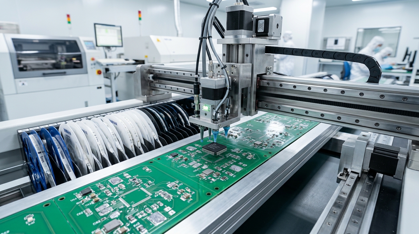
Core Principles of Surface Mount Technology.
Surface mount technology mounts parts directly onto circuit boards. In early electronics, through hole technology used long wire pins. Techs pushed leads through pre-drilled holes. That old method slowed factory output. In contrast, surface mount technology solders parts straight to copper pads. Compact surface mount devices lack long leads. Instead, they use small metal end caps or flat tabs. This shift speeds up printed circuit board assembly. It packs high logic density into small spaces. Boards run fast.
Today, smt assembly line robotics build complex gear fast. Automated smt manufacturing lines handle double-sided pcba production. Techs place tiny chip components on both sides of a bare pcb. This design cuts trace lengths. Shorter traces drop parasitic inductance and boost speed. Following sound design for manufacturability rules stops factory flaws. Teams apply design for assembly rules to boost throughput. When mixed technology assembly is needed, lines combine surface mount components with selective through hole steps. Reviewing electronic engineering technology shows how circuit plans become real factory jobs. Good dfm guidelines keep yields high.
Key Assembly Targets.
- Screen Ratio: Hold area ratio above 0.66 for clean paste release.
- Run Rate: Target 40,000 components per hour per robotic line.
- Oven State: Maintain 45 to 75 seconds time above liquidus.
- Yield Metric: Keep line yield above 99.2% first pass yield.
Panelization and Board Breakaway Design.
Factories run multiple boards in large arrays. Engineers use circuit board fabrication panelization to group small boards. Panels travel smoothly down high-speed conveyor belts. Boards link together with v scoring grooves or break away tabs. Technicians add mouse bites with small drilled holes. These tabs snap cleanly after reflow soldering. Panel rails feature global fiducials and panel fiducials. Vision cameras use these vision targets to align every print stroke. Rails keep boards flat.
Solder Paste Stencil Printing and Aperture Physics.
The assembly process starts at the stencil printer. A squeegee blade sweeps solder paste across a thin foil. The blade forces gray paste through laser cut stencil openings. Clean solder paste printing dictates the quality of every joint. In fact, most assembly defects stem from poor paste deposition. Proper squeegee pressure and controlled print speed deliver uniform brick shapes. Slow separation speed prevents paste pull-out. Good prints save cash.
Aperture Area and Aspect Ratio Rules.
Stencils rely on precise math for clean paste release. The aperture area ratio compares pad opening area to aperture wall area. Engineers insist on an area ratio above 0.66. The aspect ratio compares aperture width to stencil thickness. This aspect ratio must stay above 1.5. If walls are too deep, paste sticks inside the foil. Then pads suffer from insufficient solder. Premium stainless steel stencil foils use electropolished stencil walls. Many plants apply a nano coating to repel flux and extend the stencil wipe cycle. Clean foils stop shorts.
For fine pitch components, designers modify aperture geometries. They use a home plate aperture or windowpane pattern on large center pads. These cutouts prevent solder balls and stop solder spatter. Smart aperture reduction prevents solder bridging between close pins. Crisp pads cut flaws.
Solder Paste Chemistry and Rheology.
Solder paste combines tiny solder alloy spheres with a chemical flux vehicle. Most lead free solder lines run on sac305 alloy. This tin silver copper blend melts at 217 degrees Celsius. For older military gear, plants still use eutectic solder or tin lead solder. The flux activation removes oxides from copper pads during preheat. Plants pick no clean flux to avoid washing boards. High-reliability aerospace builds prefer water soluble flux or active rosin flux.
Paste rheology determines how paste flows under a squeegee. Quality paste exhibits thixotropic behavior. Paste viscosity drops under blade pressure, then stiffens on the pad. High slump resistance prevents wet paste from spreading across solder mask clearance dams. Techs track tack life and stencil life on the factory floor. They select type 3 solder paste for standard chips. Dense boards use type 4 solder paste or fine type 5 powder with tight powder size distribution. Good paste builds a sound intermetallic compound. Strong copper tin intermetallic layers bond each joint. Solid bonds hold tight.
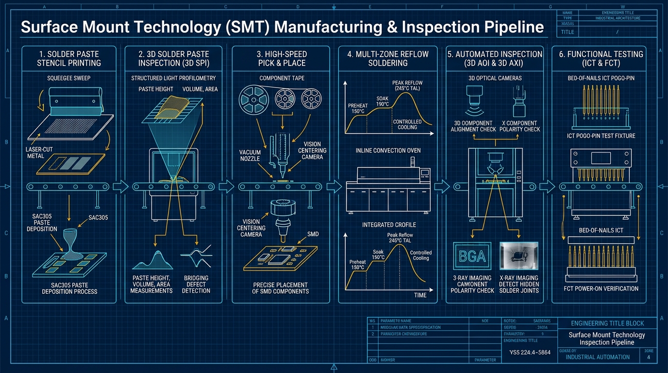
Figure 1.0: End-to-end surface mount technology workflow showing stencil paste printing, 3D SPI inspection, high-speed pick-and-place, multi-zone reflow soldering, and automated 3D optical and X-ray testing.
Solder Paste Inspection and Volumetric Control.
Boards pass directly into a 3d spi machine after printing. Solder paste inspection uses structured light lasers to map every pad. The system checks paste volume measurement, paste height, and paste area. If paste volume dips below 80 percent, the board stops. The line cleans the bare board before placement. Catching paste flaws early cuts rework costs by 90 percent. Clean boards move on.
Pick-and-Place Robotic Assembly Lines.
Once paste passes inspection, boards enter a high-speed pick and place machine. These robotic placement heads move with blistering speed. A high-yield p&p robot uses dual gantries to position thousands of parts. Robotic lines often pair a chip shooter with a flexible mounter. Both heads place chips.
Feeder Systems and Component Handling.
Feeders supply parts to the placement head. Most passive chips arrive on tape and reel packaging. The machine advances the feeder reel in tiny increments. Larger microchips arrive in a matrix tray or waffle pack. Heavy connectors feed through a vibrating tube feeder. Operators load reels while the machine runs to sustain components per hour throughput. Fast reels feed parts.
Optical Vision Centering and Nozzle Dynamics.
A vacuum nozzle picks up parts from the feeder pocket. The nozzle changer swaps tips to match part mass. High-speed cameras perform optical centering and fly by vision checks. The vision system reads the polarization mark and pin 1 indicator. It computes rotational alignment in microseconds. It checks placement accuracy before the head touches down. Controlled placement force prevents squeezing wet paste off pads. Heads place parts straight.
SMD Component Packaging and Footprint Geometry.
Surface mount devices span passive chips and complex silicon. Circuit designers must follow standard footprint design rules to ensure high yields. Good layouts save time.
Passive Chip Packages from 1206 to 01005.
Standard passive chip components include chip resistors, ceramic capacitors, and surface mount inductors. Ferrite beads filter power bus noise. Technicians measure chip size in imperial and metric codes. Early boards used large 1206 package and 0805 package parts. Later gear adopted 0603 package and 0402 package footprints. Ultra-dense devices use 0201 package and microscopic 01005 package components. These tiny mlcc capacitors demand extreme placement accuracy. Small chips fit tight.
High-Density Active IC Packages.
Active components pack millions of transistors into miniature cases. Small semiconductor packages include sot 23, sot 223, and sod 123 diodes. Integrated circuits use soic package, tssop, and msop formats with gull wing leads. High-pin processors use quad flat package, lqfp, or quad flat no lead cases. A qfn package or dfn uses bottom metal pads rather than side pins.
For high-speed compute, engineers choose ball grid array packages. A bga package features an array of small solder balls under the body. Dense chips use micro bga or chip scale package formats. Processors often sit on land grid array pads. Large chips feature thermal pads and an exposed center pad to vent heat. Reviewing our guide on integrated device technology details silicon timing and package clock pins. Designers follow ipc 7351 rules to size copper pads. They balance smd pads and nsmd pads to control stress. Good pads stop flaws.
Convection Reflow Soldering and Thermal Profiles.
Loaded circuit boards enter a multi zone oven to fuse parts to pads. Forced convection reflow blows hot gas across the board. Engineers fine-tune the thermal profile using a multi-channel thermocouple datalogger. Heat melts paste fast.
The Four Critical Reflow Zones.
A proper reflow profile balances four temperature zones:
- Zone 1 Ramp: The preheat zone warms the board at 1 to 2 degrees per second to prevent thermal shock.
- Zone 2 Soak: The thermal soak zone holds heat between 150 and 190 degrees for 60 to 120 seconds. This step equalizes thermal mass and activates flux.
- Zone 3 Peak: The reflow zone drives heat to peak reflow temperature around 245 degrees. The board spends 45 to 75 seconds in time above liquidus.
- Zone 4 Chill: The cooling zone drops heat at a cooling rate of 3 to 4 degrees per second. Fast cooling creates a fine grain joint.
Nitrogen Atmosphere and Void Reduction.
High-end lines use nitrogen reflow ovens. A nitrogen atmosphere displaces ambient air, keeping oxygen ppm below 50. Low oxygen speeds wetting and cuts oxidation. This atmosphere minimizes bga voids and promotes bright joints. In specialized low-volume jobs, vapor phase soldering provides uniform heat transfer. When mixed boards require leaded parts, plants deploy selective soldering or mini wave soldering pots. Good gas cuts voids.
Empirical Benchmarks for Surface Mount Packages.
Selecting the right package affects placement speed, thermal behavior, and defect risks. Engineers balance density against assembly tolerance. Bench tests guide line setup.
| SMD Package Type | Lead Pitch | Stencil Foil Thickness | Placement Rate | Primary Assembly Defect |
|---|---|---|---|---|
| 01005 Chip Capacitor | 0.20 mm | 0.075 mm (3 mil) | 45,000 CPH | Tombstoning and billboarding |
| 0402 Chip Resistor | 0.50 mm | 0.100 mm (4 mil) | 55,000 CPH | Component skew and misalignment |
| QFP-100 Gull Wing | 0.50 mm | 0.125 mm (5 mil) | 8,000 CPH | Solder bridging and bent leads |
| QFN-48 No-Lead | 0.40 mm | 0.100 mm (4 mil) | 12,000 CPH | Thermal pad voiding and float |
| BGA-256 Solder Ball | 0.80 mm | 0.125 mm (5 mil) | 6,000 CPH | Head-in-pillow and internal voids |
Post-Reflow Automated Inspection and Defect Control.
After exiting the cooling zone, boards undergo rigorous quality screening. Automated systems catch manufacturing errors before products ship. Fast scans find faults.
3D Automated Optical Inspection and 3D X-Ray.
Clean factories place an aoi system after reflow. High-resolution 3d aoi cameras project moire fringe patterns across the board. The system measures height, color, and joint shape. It uncovers missing parts, wrong component orientation, and defective solder fillet formation. Reading our report on automated visual inspection technology shows how machine vision models spot tiny board flaws. Optics check every lead.
Because optical cameras cannot see under bga packages, plants deploy an axi system. Automated x ray inspection generates 3d x ray computed tomography slices. Operators evaluate bga inspection images to check ball shape and measure voiding percentages. Axi systems detect dangerous head in pillow flaws and internal bridge shorts. X-rays see through chips.
Automated Test Scripting for SMT Validation.
Engineers link inspection machines to central factory servers. Automated Python scripts query inspection databases and verify lot yields using standard network protocols. Scripts track line trends.
AOI Telemetry and Defect Query Script
import requests
import json

AOI_API_URL = "http://192.168.10.50:8080/api/v1/inspection"
BOARD_SERIAL = "SN-2026-PCBA-8492"

response = requests.get(f"{AOI_API_URL}/board/{BOARD_SERIAL}")
data = response.json()

total_pads = data.get("inspected_pads", 0)
defects = data.get("defect_list", [])

print(f"Board: {BOARD_SERIAL} | Inspected Pads: {total_pads}")
if not defects:
    print("STATUS: PASS - Zero solder bridge or tombstone defects detected.")
else:
    for d in defects:
        print(f"DEFECT: Component {d['refdes']} - {d['type']} at Pad {d['pad_id']}")
Code 1.0: Python telemetry script validating post-reflow AOI defect logs.
In-Circuit and Functional Testing.
Following optical scans, boards undergo in circuit testing. A bed of nails fixture connects pogo pins to test pads. The ict fixture tests continuity and measures component values. For fast turnaround prototypes, a flying probe tester checks nets without custom jigs. Finally, functional testing powers up the board. Systems use boundary scan and jtag testing to verify microcontroller firmware. Tests prove real logic.
SMT Defect Modes and IPC-A-610 Compliance.
Controlling process drift keeps defect per million opportunities rates low. Assembly plants build boards to meet the IPC International Standards for electronic assemblies. Sound builds pass audit.
Common SMT Defects and Root Causes.
- Component Lift: Tombstoning is also called drawbridging or the manhattan effect. One end of a chip lifts off the pad. Unbalanced copper tracks or uneven paste volume cause this flaw. Proper thermal relief connections fix this issue.
- Bridge Faults: Solder bridging occurs when solder links adjacent pins, causing solder shorts. Excess paste, bent pins, or poor squeegee pressure cause bridging.
- Hidden Voids: Trapped flux gases cause voiding in thermal pads. Warped packages cause head in pillow defects where the ball touches paste but never fuses.
- Cold Joints: Insufficient reflow heat creates a dull, cold solder joint. Vibration during cooling creates a disturbed joint prone to thermal fatigue.
IPC-A-610 Acceptance Criteria.
The ipc a 610 standard sets clear rules for joint quality. Consumer gadgets follow ipc class 1 rules. Dedicated industrial gear requires ipc class 2 conformance. Mission-critical aerospace systems demand strict ipc class 3 quality. Class 3 rules mandate robust heel fillet height, minimal lead coplanarity error, and zero dewetting. Plants enforce cleanroom environment rules, esd protection, and msd handling protocols. Moisture sensitive devices undergo a mandatory bake out cycle to stop popcorning. Rules keep gear safe.
Engineering Verdict: Mastering Scalable SMT Production.
High-yield surface mount technology demands discipline across every stage. Tight stencil design, accurate solder paste printing, and closed-loop 3d spi eliminate defects early. High-speed pick and place robotics and balanced reflow thermal profiles deliver robust joints.
By pairing 3d aoi with 3d axi x-ray scans, factories protect product reliability. Applying sound dfm rules ensures high first pass yield across high-density circuit assemblies. Clean lines build great tech.